The most expensive operation in a modern AI accelerator is often not multiplication. It is moving data to the place where multiplication happens. Model weights travel between DRAM, high-bandwidth memory, caches and arithmetic units; intermediate activations make similar trips. Every transfer costs energy, consumes bandwidth and adds latency. Adding faster arithmetic units does not remove that bottleneck.
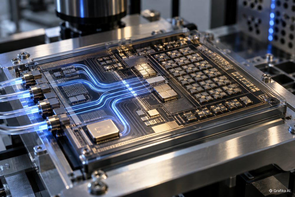
Optical neuromorphic computing attacks the problem from a different direction. Instead of treating memory, interconnect and computation as three separate blocks, researchers are developing photonic devices in which a stored physical state directly changes how light propagates. The stored state can represent a neural-network weight; an incoming optical signal carries the data; and the interaction between the two performs part of the computation.
That distinction matters. A useful photonic AI chip is not simply a processor in which copper wires have been replaced by waveguides. The more consequential architecture is one in which light transports information while the optical component itself retains the parameter needed to process that information.
Several laboratory devices can already do this. Some switch in hundreds of picoseconds. Others survive billions of programming cycles. Photonic tensor cores have demonstrated trillions of multiply-accumulate operations per second, while newer experimental architectures combine thousands of memory-like photonic neurons on one chip.
None of this means that GPUs are about to disappear. It means the boundary between processor, memory and interconnect is becoming less rigid — and that is where optical hardware becomes technically interesting rather than merely futuristic.
The real target is the memory wall, not the transistor
Neural networks spend enormous amounts of time performing matrix-vector and matrix-matrix operations. Electrically, the arithmetic is straightforward: multiply an input by a stored weight and add the result to an accumulator. At scale, however, feeding the arithmetic units becomes difficult.
A conventional accelerator must repeatedly retrieve weights from SRAM or HBM. The processor may be capable of performing enormous numbers of operations every second, but that capability becomes useless when data cannot arrive quickly enough. The problem gets worse as models become larger and accelerator clusters spread across multiple packages, boards and racks.
Photonics changes several properties at once.
First, many optical signals can travel through a waveguide simultaneously using wavelength-division multiplexing, or WDM. Different wavelengths behave like parallel information channels. Second, optical interference, attenuation and phase shifting can implement mathematical operations without reproducing every multiplication as a sequence of transistor switching events. Third, a photonic weight that remains physically programmed does not have to be loaded from external digital memory before every inference.
A 2021 integrated photonic tensor-core experiment demonstrated this idea with phase-change-material memory arrays and an optical frequency comb. The architecture performed parallel photonic in-memory computation at bandwidth above 14 GHz and reached the regime of trillions of MAC operations per second. The calculation was effectively encoded in the optical transmission of programmed devices.
The basic mechanism is easier to understand than the terminology suggests. Imagine an optical waveguide carrying an input signal. A programmable element placed on or beside that waveguide changes how much light passes through it. If its transmission represents a neural-network weight, the output optical power represents the multiplication of the input by that weight. Multiple optical channels can then be combined, allowing accumulation to occur physically.
That is analog computing. Its strength is also its weakness.
A digital multiplier is designed to return a precisely defined binary result. An optical multiplier deals with laser noise, detector noise, temperature drift, fabrication tolerances, insertion losses and imperfect programming of analog weights. When hundreds or thousands of optical elements are connected, small errors accumulate.
This is why precision matters more than spectacular peak-throughput numbers. A photonic accelerator intended for a heavily quantised inference model operating at 4 or 8 bits faces a substantially easier engineering problem than hardware expected to reproduce full floating-point training with strict numerical accuracy.
The conversion boundary matters just as much. If every operation requires a high-speed DAC before the optical core and an ADC immediately afterwards, converter power can consume a large part of the theoretical efficiency advantage. Similarly, a passive optical matrix may use little energy while the lasers, modulators, thermal stabilisation, photodetectors and control electronics around it consume much more.
So the right comparison is never “optical multiplication versus electronic multiplication.” It is complete optical subsystem versus complete electronic subsystem for the same workload, precision and accuracy target.
That is also why photonic interconnect has reached commercial engineering faster than fully optical computing. Moving bits with light is already a well-understood problem. Replacing programmable computation, state storage and nonlinear neural-network functions at the same time is considerably harder.
When the weight becomes part of the optical device
The most important component in this architecture is the photonic memory cell. It has to do two jobs that ordinary optical components do not normally perform together: retain a programmable state and use that state to modify light.
Phase-change materials were among the first convincing solutions. Materials such as GST — Ge₂Sb₂Te₅ — can switch between structural states with different optical properties. Once programmed, the material can retain its state without continuous electrical power.
An early integrated all-photonic memory demonstration stored eight distinct levels in one device, achieved switching energies down to 13.4 pJ and approached 1 GHz operating speed. Multilevel operation is particularly valuable for neural networks because a single device can represent more than a binary zero or one.
Later designs pushed individual metrics much further.
A heterogeneous silicon photonic memresonator reported in 2024 combined a metal-oxide memristor with a microring resonator. The demonstrated device reached:
-
300 ps SET time and 900 ps RESET time;
-
0.15 pJ SET energy and 0.36 pJ RESET energy;
-
approximately 2 aJ read energy in one reported measurement;
-
12 hours of demonstrated retention;
-
1,000 tested programming cycles;
-
zero static programming power between state changes.
Those numbers show exactly why benchmark tables have to be read carefully. The 0.15 pJ switching result is impressive. One thousand write cycles is not. A weight memory used mainly for inference may be rewritten relatively infrequently, so limited endurance can be acceptable. The same cell would be a poor choice for an online-learning system that updates weights continuously.
Other material systems attack that weakness.
A magneto-optic photonic memory demonstrated with cerium-substituted yttrium iron garnet, Ce, reported 1 ns programming, 143 fJ per bit and 2.4 billion programming cycles. That endurance changes the design discussion dramatically, although heterogeneous integration of magneto-optic materials brings its own fabrication and scaling complications.
A 2025 PZT optical memristor took another route. It combined non-volatile programming with fast volatile electro-optic modulation. Reported figures included a 12.3 pJ non-volatile switching energy, stability beyond 100,000 cycles, and volatile operation at 48 Gbit/s with 432 fJ per bit. That hybrid behaviour is attractive because a single device can provide a slowly changing stored parameter and a rapidly changing optical response.
And there is no requirement that every useful photonic memory must be permanently non-volatile. A 2026 neuromorphic photonic system using co-located capacitive analog memory showed why short-lived analog storage can be enough. Its architecture was evaluated against a conventional SRAM-plus-DAC approach and showed more than 26× power savings in the studied configuration. The important engineering result was that memory does not necessarily have to retain information for years. If its retention time is comfortably longer than the computation interval, refreshing it can still be cheaper than repeatedly transporting digital weights across a chip.
That changes how the specification should be written. Instead of asking for “the best optical memory,” an engineering team has to define the update pattern first.
For mostly static inference weights, prioritise retention, low read loss and zero static tuning power. For continual learning, prioritise endurance, symmetric weight updates and predictable analog programming. For temporal or spiking networks, deliberately volatile memory can become a feature because decay itself represents neural dynamics.
One of the most aggressive demonstrations appeared in 2026 with a fully in-memory photonic architecture called FLARE. The reported monolithic chip contained 7,378 photonic memory neurons, combined 7.45-second long-term retention with GHz-scale short-term dynamics, and was demonstrated in an autonomous racing-drone navigation task. Its reported system-level energy figure was 61.87 attojoules per operation for the demonstrated architecture.
That number should not be placed next to a GPU’s board-level TOPS-per-watt figure and treated as a direct comparison. Different papers count operations, optical sources, peripheral electronics and system overhead differently. This is one of the most persistent problems in unconventional-computing benchmarks. A spectacular device-level energy number says that the physical mechanism is efficient; it does not automatically tell a data-centre operator how much electricity a complete server will draw.
The practical lesson is more useful: photonic memory is no longer limited to demonstrating that a state can be stored. Researchers can now choose among competing mechanisms with radically different combinations of speed, endurance, retention, loss, programmability and manufacturing complexity.
What is likely to reach AI systems first — and what Europe can build now
The near-term AI chip is more likely to be hybrid photonic-electronic than all-optical.
Electronics remains excellent at control logic, address generation, digital storage, branching, error correction and high-precision nonlinear operations. Photonics is strongest where large quantities of data must be transported or where regular linear algebra can be mapped efficiently onto optical hardware. Forcing light to perform every task usually creates additional components without removing the underlying bottleneck.
Commercial activity already reflects that division. Optical I/O is moving towards AI packages because electrical interconnects become increasingly costly at very high bandwidths. In 2026, for example, Lightmatter reported a 1.6 Tbit/s-per-fibre demonstration using 16-wavelength DWDM, while its Passage L20 platform targets 6.4 Tbit/s in each direction and roughly 5 pJ/bit link efficiency. These are interconnect products rather than optical memory processors, but they show where photonics currently has the clearest route into high-volume AI infrastructure.
Compute will follow only when it survives a harsher checklist.
The first issue is packaging. A photonic die still needs electrical drivers, detectors, control circuitry and usually an external or integrated laser source. Fibre attachment must be repeatable at production volume. Temperature control matters because microring resonators can shift their operating wavelength as the chip heats. Laboratory probes and tunable lasers hide problems that a rack-mounted accelerator cannot.
The second issue is yield and calibration. Analog optical components fabricated nominally identically do not emerge with perfectly identical characteristics. A system containing thousands of weights therefore needs calibration, trimming or algorithms trained to tolerate hardware variations.
The third is software mapping. Existing AI stacks assume GPUs, tensor accelerators and conventional numeric formats. A photonic engine becomes useful only when models can be partitioned so that suitable layers execute optically while unsupported operations remain electronic without excessive conversion and data-transfer overhead.
Europe is unusually relevant here because integrated photonics already has an industrial and research infrastructure rather than only isolated university prototypes. The PIXEurope pilot-line programme brings together 20 institutions across 11 European countries and is building open-access capabilities spanning silicon, silicon nitride, indium phosphide, lithium niobate, hybrid integration, packaging and testing. The wider initiative has been presented with a budget of roughly €400 million.
Poland is directly inside that programme through Warsaw University of Technology, including CEZAMAT and the Institute of Microelectronics and Optoelectronics. The Polish work includes photonic integration and research involving new materials, while the programme creates a route into a wider European manufacturing chain. That is much more relevant to a Polish photonics company than trying to finance a proprietary semiconductor fab.
Even ordinary silicon-photonics prototyping is becoming easier to budget. Under the 2026 EUROPractice schedule, an imec iSiPP50G multi-project-wafer run is listed at approximately €11,000 for a 2.5 × 2.5 mm quarter block, €22,000 for a half block, and €44,000 for a 5.15 × 5.15 mm block at standard pricing, with 25 dies included. Passive silicon-photonics options start lower: about €6,700 for a half block and €12,800 for a full 5.15 × 5.15 mm block.
Those figures are fabrication prices, not complete processor-development budgets. Packaging, fibre coupling, PCB design, electronic drivers, lasers, control hardware, test equipment and engineering labour can dominate a prototype programme. A design that looks economical because its bare die fits into a €22,000 MPW slot can still become expensive once stable optical packaging is required.
That is the inconvenient part of photonic AI development: fabricating the clever structure is no longer always the hardest step. Making it repeatable, controllable and useful as a system often is.
FAQ
Will optical neuromorphic chips replace GPUs?
Not across the board. Their strongest use case is accelerating workloads dominated by highly parallel linear operations and data movement. Control logic, high-precision operations, irregular workloads and many nonlinear functions are still better handled electronically. Expect hybrid processors rather than a clean GPU replacement.
Does light make computation effectively energy-free?
No. Passive propagation can be extremely efficient, but a complete system still needs lasers, modulators, photodetectors, drivers, ADCs or DACs in many architectures, control electronics and sometimes temperature stabilisation. Any credible efficiency figure should state which of these are included.
Is the memory actually optical?
Sometimes. Phase-change cells can be written and read through optical interactions, while other architectures use an electrical memory physically integrated with an optical modulator or resonator. The important property for AI is not ideological purity; it is whether the stored weight can influence the optical computation locally without repeatedly fetching it from remote memory.
Can these chips train neural networks as well as perform inference?
Potentially, but training places much tougher requirements on memory endurance and weight-update accuracy. A cell that survives only thousands of programming cycles may be adequate for relatively static inference weights and completely unsuitable for intensive on-chip training. Training also magnifies analog precision and calibration problems.
Why use analog computation when digital AI hardware is so mature?
Because matrix operations map naturally onto physical optical processes and can run massively in parallel. The price is reduced numerical determinism. The technology becomes attractive when the workload tolerates limited precision and when the energy saved in data movement exceeds the cost of optical conversion and control.
What is the biggest remaining technical problem?
There is no single device-level metric left to fix. The difficult problem is simultaneously achieving low optical loss, sufficient analog precision, high write endurance, long-enough retention, temperature stability, good fabrication yield and manufacturable packaging. Improving one metric while sacrificing three others does not produce a commercial accelerator.
When should a company seriously consider photonic neuromorphic hardware?
When profiling shows that memory bandwidth or interconnect energy is limiting the workload, the important mathematical kernels are regular and parallel, and the model can tolerate reduced precision. If the existing bottleneck is software, small batch sizes, control flow or poor utilisation of conventional accelerators, replacing electronics with photonics is solving the wrong problem.
The first action should therefore be a data-movement audit, not a photonic-chip design. Measure how many bytes are transferred for each useful MAC, where weights reside during inference, how often those weights are rewritten, what precision the model genuinely needs and how much energy is consumed by memory and interconnect rather than arithmetic. Only after those numbers are known should a photonic architecture be evaluated. And the first design mistake to eliminate is comparing a laboratory optical core with a complete GPU: include lasers, converters, drivers, memory, calibration and packaging on both sides. If the advantage survives that comparison, the project has a technical reason to exist.